• Skip to main content
  • Skip to secondary menu
  • Skip to primary sidebar
  • Home
  • About
  • Contact Us
  • Tip News!

Sammy Hub

Ultimate resource for all Samsung news, leaks, reviews

  • Phones
  • Tablets
  • Wearables
  • TV
  • Hardware
    • Components
    • Storage
    • Monitor
  • Software
  • Tech
  • Home Appliance
You are here: Home / Latest / Samsung completes 5nm FinFET process development

Samsung completes 5nm FinFET process development

April 16, 2019 By Siddhanth Leave a Comment

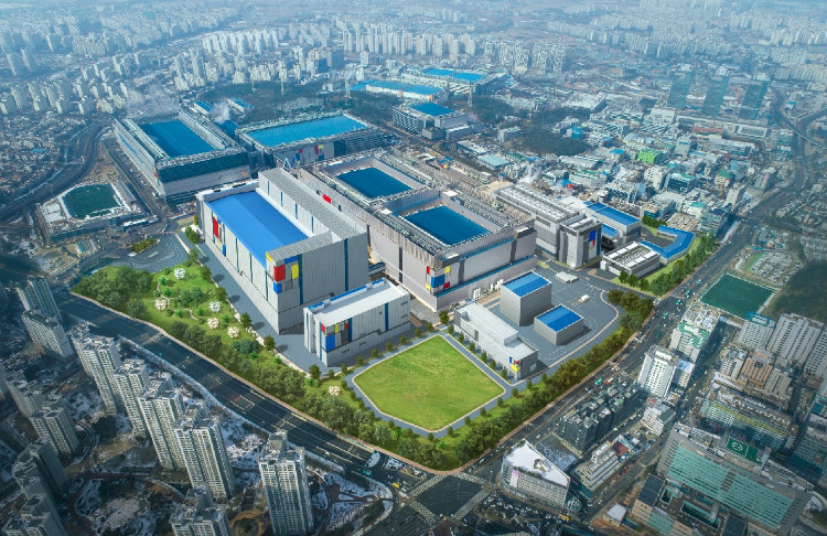
Samsung has announced the completion of its 5nm FinFET process technology, expanding its extreme ultraviolet (EUV)-based process portfolio. Samsung claims its 5nm FinFET process offers 10 percent improvement in performance with 20 percent lower power consumption when compared to 7nm chipsets, further helped by the EUV lithography that “reduces mask layers while providing better fidelity.”

Samsung is also quick to point out that its 5nm process can reuse 7nm intellectual property (IP), thus helping its customers to reduce product development time and migration costs.

While chipsets with 5nm process is still under sampling, they are collaborating with customers on 6nm with a product that has already been taped-out of its 6nm process.

Reader Interactions

Leave a Reply Cancel reply

Your email address will not be published. Required fields are marked *

Primary Sidebar

Search

Subscribe Now!

Recent Stories

Galaxy A17 5G with Troomi OS

Samsung Galaxy A17 5G Gets Troomi OS for Kid-Safe Experience 

Samsung Ultra Slim Laptop OLED Display at the Computex 2026

Samsung Showcases Ultra Slim Laptop OLED Panel at Computex 2026

Samsung HBM4E

Samsung Ships Industry-First HBM4E Samples to Global Customers

Samsung announces development of 4K 360Hz QD-OLED panel

Samsung Unveils World’s First 4K 360Hz QD-OLED Monitor Panel

Sleep Apnea Detection on Galaxy Watch

Samsung Partners With MGH to Study GLP-1 Muscle Loss Monitoring

Copyright © 2026 · Sammy Hub