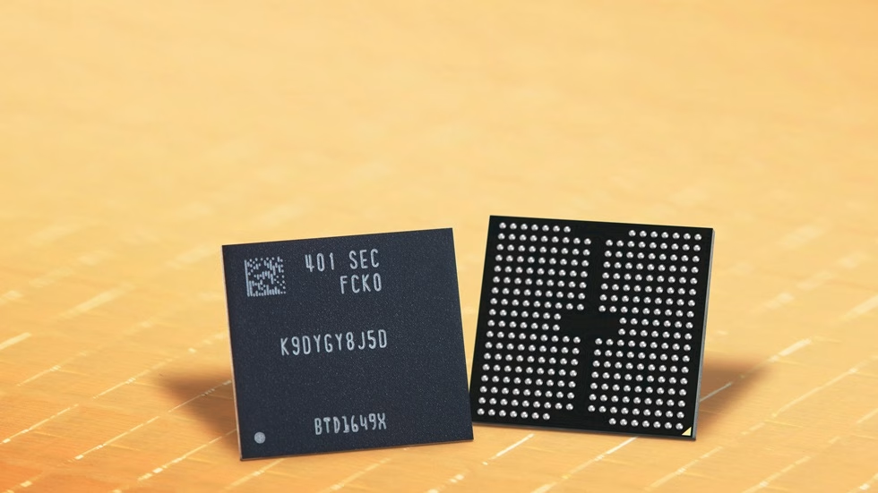
Samsung has successfully built a pre-production 900-layer-class V-NAND chip, making the Korean giant the first company in the world to reach this milestone. According to a report by ETNews, Samsung used its Cell Multi Bonding (CMB) technology to bond two 450-layer cell wafers into a single integrated system.
A core component in AI servers, smartphones, and data centre SSDs, NAND flash with higher layer counts allows more data to be packed into the same chip area while improving power efficiency, making stacking depth a key competitive metric in AI infrastructure.
Samsung confirmed that the prototype passed functional validation, stating that “normal cell operation characteristics were verified,” indicating the chip operates beyond a theoretical stack.
To reach 900 layers, Samsung addressed two technical obstacles: wafer warpage and bonding misalignment. The company resolved warpage through an advanced upper chuck design and corrected misalignment using an overlay correction technique. New bitline and wordline structures also reduced both power consumption and chip size.
Currently, SK Hynix leads the industry with 321-layer 4D NAND, but Samsung is separately preparing volume production of its 10th-generation V-NAND (V10, 400+ layers) this year. On the research front, China’s YMTC is approaching the 300-layer threshold in mass production.
According to an industry expert, the 900-layer achievement sends a signal to global customers that Samsung still retains its technology lead. There’s no information on when this tech will enter mass production.
Leave a Reply