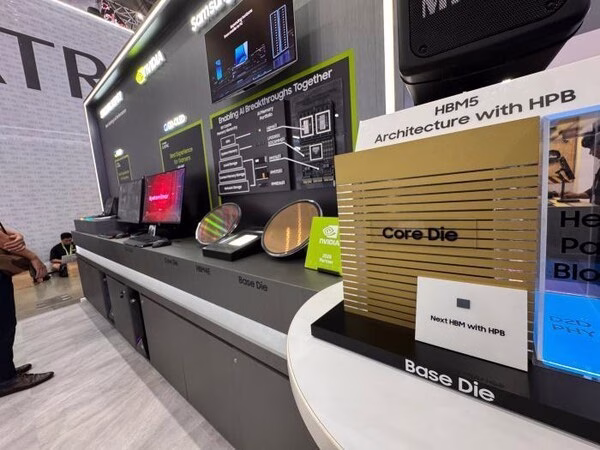
Samsung has unveiled the first physical mockup of its eighth-generation high-bandwidth memory, HBM5, at the ongoing Computex 2026 in Taipei. The display, held within the Samsung Display booth, paired the next-generation AI memory with a new in-package thermal structure called Heat Path Block, or HPB.
HPB addresses heat buildup at the die-to-die interface — the high-speed link between the HBM base die and the GPU — where power density rises as stacks grow taller and run faster. “It is a,” said
Song Jae-hyuk, president and CTO of Samsung’s Device Solutions division, mentions it has a “chimney-like structure that adds additional thermal pathways to reduce thermal resistance and improve operational stability”.
HBM5 will also adopt a base die manufactured on Samsung’s in-house 2nm foundry process, down from the 4nm node used across HBM4 and HBM4E. Samsung also displayed HBM4E wafers at Computex.
Rival SK hynix is pursuing the same thermal bottleneck via a different method. Its iHBM design embeds electrically non-conductive, thermally conductive silicon elements directly into the D2D PHY layer, cutting thermal resistance by more than 30% against current products. Neither company expects either design to reach mass production before 2028.
Leave a Reply