UPDATE: You can now find the presentation deck (PDF) of Samsung explaining 3D V-NAND at the Flash Memory Summit. Click here
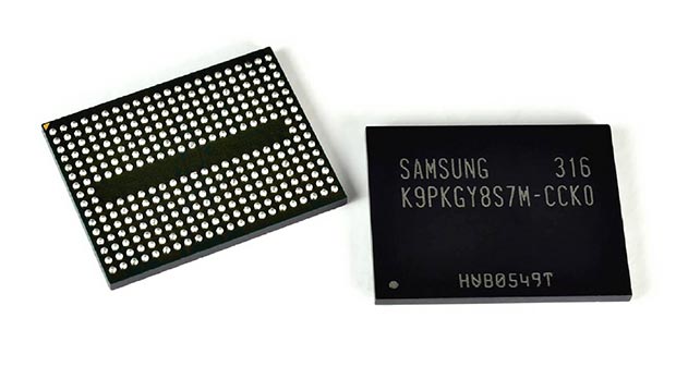
Samsung has announced the mass production of the industry’s first 3D Vertical NAND (V-NAND) flash memory. Today’s flash memory manufacturing process technology has reached to 10nm-class and given the flash memory based on planar structure, Samsung recognised the issue of scaling limit due to cell-to-cell interference. But with the V-NAND, Samsung says the new NAND flash memory can scale the limit of existing NAND flash technology and gain in performance and area ratio.
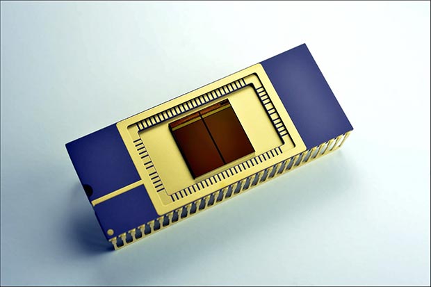
The new 3D V-NAND will be used in enterprise solutions, embedded NAND storage and solid state drives (SSDs) and as a start Samsung is mass producing a 128Gb (16GB) V-NAND. The chip takes advantage of Samsung’s vertical cell structure based on 3D Charge Trap Flash (CTF) technology and vertical interconnect process technology to link the 3D cell array, which when combined offers twice the scaling of 20nm-class NAND flash available today.
Samsung has promised to launch new 3D V-NAND products with improved performance and higher density in the future. As for how Samsung achieved this, Samsung has given a detailed technical explanation below.

Samsung’s new V-NAND solves such technical challenges by achieving new levels of innovation in circuits, structure and the manufacturing process through which a vertical stacking of planar cell layers for a new 3D structure has been successfully developed. To do this, Samsung revamped its CTF architecture, which was first developed in 2006. In Samsung’s CTF-based NAND flash architecture, an electric charge is temporarily placed in a holding chamber of the non-conductive layer of flash that is composed of silicon nitride (SiN), instead of using a floating gate to prevent interference between neighboring cells.
By making this CTF layer three-dimensional, the reliability and speed of the NAND memory have improved sharply. The new 3D V-NAND shows not only an increase of a minimum of 2X to a maximum 10X higher reliability, but also twice the write performance over conventional 10nm-class floating gate NAND flash memory.
Also, one of the most important technological achievements of the new Samsung V-NAND is that the company’s proprietary vertical interconnect process technology can stack as many as 24 cell layers vertically, using special etching technology that connects the layers electronically by punching holes from the highest layer to the bottom. With the new vertical structure, Samsung can enable higher density NAND flash memory products by increasing the 3D cell layers without having to continue planar scaling, which has become incredibly difficult to achieve.
Leave a Reply